


ADUM2401CRIZ-RL
Description
Technical Parameters
Shenzhen MATCHINGIC Technology Co., Ltd: Your Professional Digital Isolators Supplier
Shenzhen MATCHINGIC Technology Co., Ltd was founded in 2010, the company always adhere to the concept of talent is the company's wealth, in the years of market honed, formed a group of enterprising, innovative staff, while expanding its market share at home and abroad, the company continues to optimize internal business processes, improve international sales and procurement business, adhere to the original goods only, deepen the level of customer service, gradually formed its own industry advantages.
Why Choose Us
Quality products
Our products are of high quality and meet all the required industry standards. We use advanced technology and modern equipment to ensure that our products are of the highest quality.
Quick turnaround time
We has a streamlined production process that ensures quick turnaround times. We can quickly produce and deliver to customers, making them an excellent choice for projects with tight deadlines.
Professional team
We has a team of highly skilled technical professionals who are always ready to assist with any technical issues that customers may have. The factory provides comprehensive technical support, including design support, product selection, and application support.
Quality services
We provide high-quality services that meet the highest industry standards. We follow best practices in our work processes and adhere to strict quality control measures to ensure that we deliver the best results to our clients.


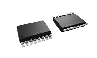


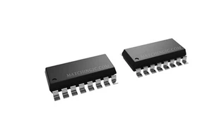
Channel digital isolators are electronic components that are used to provide electrical isolation between two circuits. They essentially act as a barrier that prevents the passage of electrical energy or data between the two circuits. They consist of a signal transmitter, a signal receiver, and an isolation barrier that separates the two. The isolation barrier is usually made up of a dielectric material or a magnetic field, and it does not allow electrical or data signals to pass between the two channels.

Advantages of Channel Digital Isolators


1. High signal integrity: Channel digital isolators provide a high level of signal integrity and accuracy that is important in applications such as data acquisition, instrumentation, and control.
2. Enhanced safety: Channel digital isolators provide galvanic isolation, which is essential in high voltage applications, thus reducing the risk of electric shocks, ground loops, and voltage spikes.
3. Reduced system noise: Channel digital isolators help reduce system noise caused by electromagnetic interference (EMI), radio frequency interference (RFI), and ground loops. This, in turn, enhances the quality and reliability of the system signals.
4. Small form factor: Channel digital isolators are available in a wide range of compact, surface-mount packages, making them suitable for use in applications where space is limited.
5. Low power consumption: Channel digital isolators are designed to consume low power, which makes them ideal for use in portable and battery-operated applications.
6. High-speed data transfer: Channel digital isolators provide fast and reliable data transfer without any loss of information, which is essential in applications such as USB, Ethernet, and SPI.
7. Cost-effective: Channel digital isolators are a cost-effective alternative to traditional optocouplers. They are also more reliable, have a longer lifespan, and are more resistant to temperature fluctuations and aging.

Channel digital isolators are most commonly used when potential ground differences are present. Sensor inputs can operate at varying voltages, ranging from as low as 3 volts to 48 volts or higher, and a digital isolator helps provide for this type of application.
For example, if the microprocessor is operating at 3.3 volts and the inputs range from 24 volts to 48 volts, this could cause a significant potential difference in ground voltages, which can introduce damaging voltage levels to the devices present, skew sensor data, and introduce errors. Some form of isolation is needed to ensure accuracy. The sensor signal is usually conditioned by filters, protection circuits, an amplifier, and digitized by an ADC. This is the data signal that's needed by the PLC processor to function.
A digital isolator is used to eliminate any errors due to ground loops. And it's desirable for the digital isolator to have a low latency or propagation delay, low noise, and a high data rate. In effect, the less a digital isolator is visible to the input signal, the better.
Measurement devices used in industrial environments often require isolation for user and system safety, and to ensure accurate measurements in the presence of high common-mode voltages. Digital isolators offer a reliable and easy to use alternative to older technologies such as optocouplers. Utilizing digital isolators, engineers can optimize isolated system designs for reduced power consumption and guaranteed system performance without resorting to excessive design margin to make up for missing or incomplete device specifications.
Isolation amplifiers were an initial solution to this problem, but have been outdated with the need for measurements with higher bandwidth and resolution. Today, the most accurate, economical, and efficient technique for performing these measurements is to isolate the entire measurement front end, including the analog-to-digital converter (ADC), and to implement an isolated serial link to the rest of the system.
Up until about ten years ago, optocouplers were one of the few practical solutions for isolating digital signals. However, ask any engineer who has had to design with them, and you will quickly learn how challenging it is to develop an efficient and reliable system, especially when trying to keep costs to a minimum. Optocouplers use an LED to generate light across an isolation barrier to turn a phototransistor on and off. When designing with optocouplers, you have to guarantee that the LED will generate enough light to turn on the receiving phototransistor, and that the output rise and fall times will be fast enough to support operation at the desired frequency. One of the most important optocoupler specifications is the current transfer ratio. The CTR is the ratio of the collector current that appears at the phototransistor to the current through the LED
Measurement devices used in industrial environments often require isolation for user and system safety, and to ensure accurate measurements in the presence of high common-mode voltages. Digital isolators offer a reliable and easy to use alternative to older technologies such as optocouplers. Utilizing digital isolators, engineers can optimize isolated system designs for reduced power consumption and guaranteed system performance without resorting to excessive design margin to make up for missing or incomplete device specifications.
Isolation amplifiers were an initial solution to this problem, but have been outdated with the need for measurements with higher bandwidth and resolution. Today, the most accurate, economical, and efficient technique for performing these measurements is to isolate the entire measurement front end, including the analog-to-digital converter, and to implement an isolated serial link to the rest of the system.
When isolated measurement systems use high sample rates, isolating a serial bus with optocouplers can become a daunting task. The parasitic capacitance of the receiver photodiode limits the speed at which an optocoupler can pass digital signals. You can charge this parasitic capacitance faster by increasing the amount of light coming from the LED, but this increases power consumption. In addition, few optocouplers offer more than two channels per package, only in the same direction, and do not typically include timing specifications related to channel-to-channel matching. While it is logical to assume good matching between optocouplers in the same package, not having a printed specification means you must make an engineering assumption. As is the case when relying on unprinted specifications, most prudent engineers will opt to leave ample design margin, operating at a much lower performance than a data sheet would indicate when considering a single optocoupler.
How Does a Channel Digital Isolator Work
Channel digital isolators couple data across an isolation barrier. This is achieved by using a modulator to transmit high frequency carrier across the barrier to represent either a high or low digital state and no signal to represent the other state. The receiver demodulates the signal after advanced signal conditioning to produce an isolated output through a buffer stage.
Channel digital isolators use single-ended CMOS or TTL logic switching technology. The voltage range normally ranges from 3 volts to 5.5 volts for both supplies, VCC1 and VCC2, though some devices may support a larger supply voltage range. When designing the digital isolators, it is important to keep in mind that due to the single-ended design structure, digital isolators do not conform to any specific interface standard and are only intended for isolating single-ended digital signal lines.
Careful consideration of layouts should be used when using a digital isolator. A minimum of four layers is required to accomplish a low EMI PCB design.
Layer stacking should be in the following order from top to bottom:
● High-speed signal layer
● Ground plane
● Power plane
● Low frequency signal layer
Routing the high-speed traces on the top layer avoids the use of vias and the introduction of air inductances and allows for clean interconnects between isolator and the transmitter and receiver circuits of the data link.
Placing a solid ground plane next to the high-speed signal layer establishes controlled impedance for transmission light interconnects and provides excellent low inductance path to the return current flow. Placing the power supply next to the ground plane creates an additional high frequency bypass capacitance. Routing the slower-speed control signals on the bottom layer allows for greater flexibility, as these signal lengths usually have margin to tolerate discontinuities such as vias.
If an additional supply voltage plane or signal layer is needed, add a second power or ground plane system to the stack to keep it symmetrical. This makes the second mechanically stable and prevents it from warping. Also, the power and ground plane at each power system can be placed closer together, thus increasing the high frequency bypass capacitance significantly.
Why Do Channel Digital Isolator Need Isolated Power?
Because each side of the device must have power for both the internal and there is no physical link between the two, digital isolators require a separate power supply on the primary and secondary sides. This criterion applies to channel digital isolators and isolated devices with integrated interfaces, regardless of whether the device provides basic or reinforced isolation.

The supply voltages VCC 1 and VCC 2 determine the digital isolator's input and output signal voltages. From device to device, the exact relationship to VCC will differ. It is advisable to keep supplies similar to the isolated power supply voltage to guarantee that the output of the digital isolator is optimum for the logic levels of interfacing components.

The MCU signals must operate at 5-volt logic levels when employing a digital isolator powered by 5 volts and interfaced to an MCU. A digital isolator can be powered from a variety of sources.
What is CMTI and How Does It Affect Digital Isolation?

The maximum tolerated rate of rising or falling of the common-mode voltage applied between two isolated circuits is common-mode transient immunity or CMTI. The two isolated circuits concerning digital isolators are the transmit and receive sides of the isolator, internal to the digital isolator.
The maximum tolerated rate of rising or falling of the common-mode voltage applied between two isolated circuits is common-mode transient immunity or CMTI. The two isolated circuits concerning digital isolators are the transmit and receive sides of the isolator, internal to the digital isolator.

How are Capacitive Channel Isolators Built?
Channel digital isolators comprise two independent integrated circuit or IC chips-an input circuit and an output circuit-joined by bond wires and a high-quality, high-voltage resistant mold compound. The digital isolator is illustrated in cross-section and as an x-ray.
A double or single silicon dioxide type of capacitive barrier can be used as the insulator in a digital isolator circuit, and both can resist very high voltage levels by design. The capacitive-based ice is built of the semiconductor industry's highest dialectic strength type of material. It's made in a cleanroom wafer fab with low variation from component to part.
The primary contributors to isolation performance are the technology itself and the design architecture due to the tightly controlled manufacturing environment and the quality of the silicon dioxide dielectric. On-off keying, and edge-based modulation designs were commonly used in capacitive isolators. Both terms refer to the timing strategies that are employed to initiate an output change.
Data transmission is started with an input pulse of a specific duration in an edge-based digital isolator like the one shown below.
A single-ended input signal entering the high-frequency channel is split into a differential signal by the inverter gate at the input. The signal is then differentiated into transient pulses by the capacitor resistor networks. The durations between signal transients are measured by decision logic at the output of the high-frequency channel comparator.
The decision logic compels the output multiplexer to switch from high frequency to low-frequency channel if the delay between two successive transients exceeds a specified time limit, as in a low-frequency signal.
Low-frequency signals are pulse-width modulated with an internal oscillator's carrier frequency to create a high-frequency signal that can pass through the capacitive barrier. With a time basis typically in the tens of nanoseconds, the oscillator is used to set the timescale of the DC PWM channel. The PWM communication is then packetized, with the smallest packets feasible being higher than the oscillator frequency.
The edge-based isolator is built so that the oscillator frequency does not show up in the output spectrum. Because the input is modulated, a low pass filter is required to separate the high-frequency carrier from the actual data before it is passed to the output multiplexer and output pins, resulting in the electrical isolation of the digital input signal.
FAQ
Hot Tags: adum2401criz-rl, China adum2401criz-rl manufacturers, suppliers, ADUM140E1WBRWZ-RL, ADUM1447ARQZ-RL7, ADUM1300WSRWZ-RL, ADUM142E1BRWZ-RL, ADUM1440ARQZ-RL7, ADUM110N1BRZ-RL7
Previous
ADUM2200BRIZ-RLNext
ADUM2200ARWZ-RLSend Inquiry
You Might Also Like


